- 您现在的位置:买卖IC网 > Sheet目录1219 > HIP6500BEVAL1 (Intersil)EVALUATION BOARD HIP6500
�� �
�
�Application� Note� 9862�
�State� Transitions�
�Figure� 6� shows� the� transition� from� active� state� (S0,� S1)� to� S3�
�sleep� state� on� the� HIP6500BEVAL1� board.� Prior� to� time� T0,�
�the� evaluation� board� was� operating� in� active� mode,� with� SW1�
�on� and� SW2� and� SW3� off.� At� time� T0,� SW2� is� switched� on,�
�5V� DUAL�
�triggering� the� turn-off� of� the� ATX� and� the� switch-over� of� the�
�output� regulation� from� the� active� ATX� output� rails� to� the� 5VSB�
�supply.� Very� shortly� after� time� T0,� the� ATX� responds� to� the�
�turn-off� request,� and� the� 5V� input� starts� to� ramp� down� under�
�the� current� drawn� by� the� embedded� 5� Ω� serpentine� resistor.�
�As� it� can� be� noticed� in� the� scope� capture,� the� transitions� are�
�devoid� of� any� perturbations.� These� smooth� transitions� are�
�desirable� in� a� computer� system,� power� glitches� being� the�
�leading� cause� of� power-related� system� crashes.�
�GND>�
�3.3V� DUAL/SB�
�3.3V� MEM�
�2ms/DIV�
�5VIN�
�2.5V� MEM�
�2.5V� CLK�
�T0�
�FIGURE� 7.� HIP6502BEVAL1� ACTIVE� STATE� (S0,� S1)� TO�
�3.3V� DUAL�
�3.3V� SB�
�5VIN�
�2.5V� MEM�
�5V� DUAL�
�2.5V� CLK�
�STANDBY� STATE� (S3)� TRANSITION� WITH� ALL�
�OUTPUTS� ENABLED�
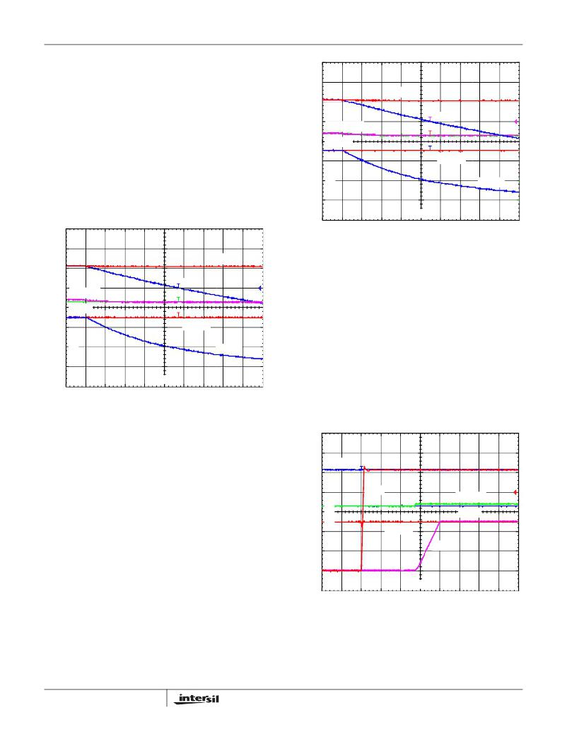
�Figure� 8� highlights� the� transition� back� from� S3� sleep� state� to�
�active� state� (S0,� S1)� with� all� outputs� enabled,� as� captured� on�
�the� HIP6500BEVAL1� board.� At� time� T0,� SW2� is� switched� off,�
�enabling� the� main� ATX� outputs.� As� 3.3VIN,� 5VIN,� and� 12VIN�
�exceed� their� undervoltage� thresholds,� the� 25ms� timer�
�internal� to� the� HIP6500B� is� initiated.� At� T1� the� time-out�
�GND>�
�2ms/DIV�
�expires,� conduction� on� the� 3.3V� DUAL� and� 5V� DUAL� outputs� is�
�transferred� to� the� N-MOS� switches� and� the� 2.5V� CLK� output�
�begins� its� ramp-up.� At� time� T2,� all� the� outputs� are� functional�
�T0�
�FIGURE� 6.� HIP6500BEVAL1� ACTIVE� STATE� (S0,� S1)� TO�
�STANDBY� STATE� (S3)� TRANSITION� WITH� ALL�
�OUTPUTS� ENABLED�
�Figure� 7� shows� the� transition� from� active� state� (S0,� S1)� to� S3�
�sleep� state� on� the� HIP6502BEVAL1� board.� Similarly,� this�
�board� mirrors� the� functionality� and� benefits� of� the�
�HIP6500BEVAL1.�
�and� ready� for� active� state� operation.� The� 2.5V� MEM� output� is�
�maintained� glitch-free� throughout� the� input� voltage� transition�
�from� the� standby� to� the� main� ATX� outputs.�
�5V� DUAL�
�5VIN�
�3.3V� DUAL�
�3.3V� SB�
�2.5V� MEM�
�2.5V� CLK�
�GND>�
�10ms/DIV�
�T0�
�T1�
�T2�
�FIGURE� 8.� HIP6500BEVAL1� STANDBY� STATE� (S3)� TO�
�ACTIVE� STATE� (S0,� S1)� TRANSITION� WITH� ALL�
�OUTPUTS� ENABLED�
�5�
�发布紧急采购,3分钟左右您将得到回复。
相关PDF资料
HIP6501AEVAL1
EVALUATION BOARD ACPI HIP6501
HIP9011EVAL1Z
BOARD EVALUATION FOR HIP9011
HM2H08P115LF
HM2H08P115LF SHROUD STYLE B LF
HM2P12P1LF
HM2 M INS STYLE N WIDE
HM2R06P1LF
MILLIPACS RCP HSG
HM2SC22A8
HM2SC22A8-MILLIPACS 2R SHIELDING
HM2SC22B
HM2SC22B-MPACS SHIELD COVERS
HMC6352-DEMO
DEMONSTRATION BOARD FOR HMC6352
相关代理商/技术参数
HIP6500CB
制造商:Rochester Electronics LLC 功能描述:- Bulk
HIP6500CB-TS2490
制造商:Rochester Electronics LLC 功能描述:- Bulk
HIP6500EVAL1
制造商:INTERSIL 制造商全称:Intersil Corporation 功能描述:Multiple Linear Power Controller with ACPI Control Interface
HIP6501
制造商:INTERSIL 制造商全称:Intersil Corporation 功能描述:Triple Linear Power Controller with ACPI Control Interface
HIP6501A
制造商:INTERSIL 制造商全称:Intersil Corporation 功能描述:Triple Linear Power Controller with ACPI Control Interface
HIP6501A_04
制造商:INTERSIL 制造商全称:Intersil Corporation 功能描述:Triple Linear Power Controller with ACPI Control Interface
HIP6501ACB
功能描述:IC PWM TRIPLE POWER CTRLR 16SOIC RoHS:否 类别:集成电路 (IC) >> PMIC - 电源控制器,监视器 系列:- 产品培训模块:Lead (SnPb) Finish for COTS
Obsolescence Mitigation Program 标准包装:2,500 系列:- 应用:多相控制器 输入电压:- 电源电压:9 V ~ 14 V 电流 - 电源:- 工作温度:-40°C ~ 85°C 安装类型:表面贴装 封装/外壳:40-WFQFN 裸露焊盘 供应商设备封装:40-TQFN-EP(5x5) 包装:带卷 (TR)
HIP6501ACB-T
功能描述:IC PWM TRIPLE POWER CTRLR 16SOIC RoHS:否 类别:集成电路 (IC) >> PMIC - 电源控制器,监视器 系列:- 产品培训模块:Lead (SnPb) Finish for COTS
Obsolescence Mitigation Program 标准包装:2,500 系列:- 应用:多相控制器 输入电压:- 电源电压:9 V ~ 14 V 电流 - 电源:- 工作温度:-40°C ~ 85°C 安装类型:表面贴装 封装/外壳:40-WFQFN 裸露焊盘 供应商设备封装:40-TQFN-EP(5x5) 包装:带卷 (TR)